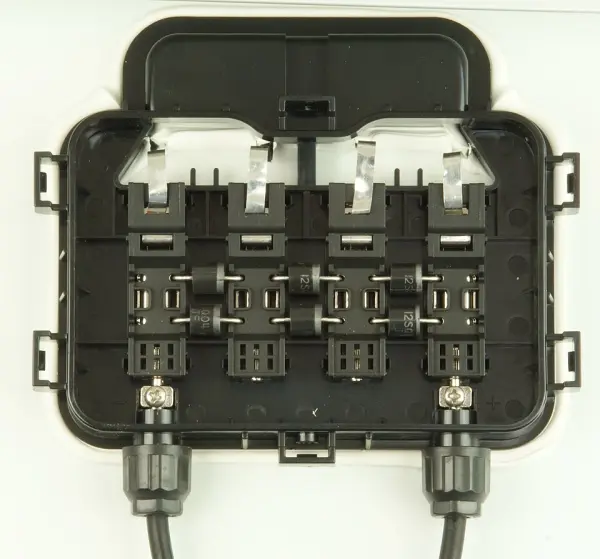
Direct Answer: To perform solar panel bypass diode testing, disconnect the module and set a digital multimeter to diode test mode. Place the red lead on the anode and black lead on the cathode; a healthy Schottky diode reads 0.30V to 0.45V forward drop. Reverse the leads; the meter must read “OL”. A 0.00V reading in both directions indicates a shorted diode causing a 33% string voltage collapse.
Engineering Principle: Accurate solar panel bypass diode testing isolates defective silicon junctions that siphon up to 66% of array harvest, turning destructive cell reverse-bias hot spots into harmless, low-impedance bypass loops.
When an off-grid solar array displays an unexplained drop in energy production, field technicians often suspect battery degradation, charge controller maximum power-point tracking (MPPT) malfunction, or persistent soiling. However, in dozens of field autopsies across residential and remote industrial arrays, the true culprit is concealed inside the module rear junction box: a short-circuited or blown-open bypass diode. Photovoltaic bypass diodes are the silent sentinels of solar arrays. Under uniform solar irradiance, they remain completely inactive, presenting an open circuit that allows photogenerated direct current to travel unimpeded down the series cell strings. Yet when a single fallen leaf, chimney shadow, or localized layer of bird droppings shades even one photovoltaic cell, that unshaded string forces current through the high-impedance shaded cell, driving it into severe reverse bias.
Without functional bypass protection, the reverse-biased cell acts as an electrical resistor rather than an electrical generator, dissipating string wattage as concentrated thermal heat. This localized thermal concentration can exceed 150°C, triggering hot-spot thermal runaway, backsheet delamination, glass shattering, and permanent cell destruction. To prevent catastrophic failure, modern photovoltaic modules incorporate three or more bypass diodes that safely shunt current around shaded cell groups. When these semiconductor devices fail, systematic solar panel bypass diode testing provides the only reliable diagnostic method to confirm whether a module requires junction box servicing, Schottky diode replacement, or warranty decommissioning.
Table of Contents
- 1. The Physics of Cell Reverse-Biasing and Hot-Spot Runaway
- 2. Bypass Diode Architecture: 3-Diode Substrings and Conduction Curves
- 3. Diagnostic Matrix: Shorted vs. Open-Circuit Diode Signatures
- 4. Interactive Solar Panel Bypass Diode Diagnostic Calculator
- 5. Step-by-Step Multimeter SOP: Bench Diode Test Mode Protocol
- 6. Non-Invasive Sunlight Field Audit: The Voc Drop and Shadow Test
- 7. NREL Infrared Thermography Standards: FLIR Diagnostic Thresholds
- 8. Junction Box Servicing: Schottky Sizing, Soldering and IP67 Sealing
- 9. Authoritative Engineering References
- 10. Frequently Asked Questions (FAQ)
1. The Physics of Cell Reverse-Biasing and Hot-Spot Runaway
To master the diagnostics behind solar panel bypass diode testing, an electrical engineer must first examine the solid-state physics of a series-connected photovoltaic circuit. A standard 60-cell monocrystalline module consists of 60 individual p-n junction silicon wafers connected in electrical series. Under standard test conditions (STC: 1,000 W/m² solar irradiance, 25°C cell temperature, AM 1.5 spectrum), each individual cell generates approximately 0.55V to 0.62V at its maximum power point (Vmp) and delivers an operating current (Imp) of 9A to 11A. Because every cell is in series, Kirchhoff’s Current Law dictates that the exact same current must pass sequentially through every single wafer in the string.
When an obstruction covers a single cell, that cell can no longer generate its rated photogenerated current (Iph). Its internal photocurrent plunges to near zero. However, the remaining 59 unshaded cells in the string continue to produce full current. These healthy cells act as an external current generator, forcing string amperage through the shaded wafer. Because the shaded cell cannot generate this current through normal photovoltaic action, the current forces the p-n junction into reverse bias, driving its operating voltage deeply negative (Vcell < 0V).
As the reverse voltage across the shaded cell escalates, the electrical power dissipated within the cell silicon transitions from positive energy generation to negative resistive heating. The power dissipation formula is expressed as:
P_diss = I_string × |V_reverse|
In a module lacking bypass protection, the reverse voltage across a single shaded cell can reach the cumulative open-circuit potential of the remaining series cells in the sub-string, climbing as high as 15V to 24V. At a standard string current of 10A, this produces an internal power dissipation of 150W to 240W concentrated entirely within a wafer area of approximately 156 mm by 156 mm. This thermal concentration generates localized temperatures exceeding 160°C. Within minutes, the ethylene vinyl acetate (EVA) encapsulant browns and outgasses, the fluoropolymer backsheet bubbles and chars, internal solder joints melt, and thermal stress fractures the front tempered glass sheet.
Sandia National Laboratories — Stand-Alone PV Simulation Performance (SAND87-2379 / OSTI ID: 6207302)
Sandia empirical modeling of stand-alone arrays under partial shading confirms that without bypass diode action, a single shaded cell drops the entire array voltage by an amount proportional to cell breakdown voltage, forcing the battery charging current to bypass normal MPPT tracking. When a bypass diode conducts, the string voltage is preserved with only a minor forward voltage penalty (Vf ≈ 0.35V to 0.45V), eliminating destructive localized cell heating while maintaining system charging continuity.
2. Bypass Diode Architecture: 3-Diode Substrings and Conduction Curves
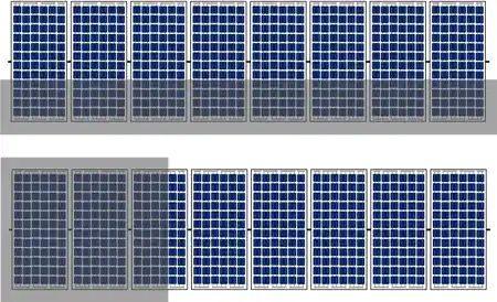
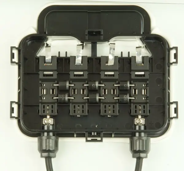
To eliminate localized thermal destruction while minimizing manufacturing complexity, the global photovoltaic industry established the 3-diode architectural standard. Rather than installing a costly diode across every individual cell, manufacturers partition the module into three series-connected cell groups known as substrings. In a standard 60-cell panel, each substring contains 20 cells; in a 72-cell module, each substring contains 24 cells. In modern 120-cell and 144-cell split-cell (half-cut) modules, twin parallel substrings share three miniature surface-mount or axial Schottky diodes housed inside three separate split junction boxes located along the panel center spine.
The bypass diode is wired in anti-parallel (reverse polarity) across each substring. Under unshaded conditions, each 20-cell substring generates approximately 11V to 13V of positive potential. Because the diode cathode is connected to the positive terminal of the substring and the anode is connected to the negative terminal, the diode is reverse-biased by 11V to 13V. In this reverse state, the diode allows only a minuscule parasitic leakage current (typically less than 20 microamps) to escape, allowing 99.99% of generated power to travel down the DC output cables to your off-grid charge controller.
When shading occurs on any cell within Substring 1, that cell reverse-biases. As the negative voltage on the shaded wafer grows, the net potential of the entire 20-cell substring collapses from positive 12V down through 0V and into negative polarity. The moment the substring potential drops below negative 0.35V, the anti-parallel bypass diode becomes forward-biased. The diode immediately transitions into conduction mode, providing an ultra-low-resistance bridge that shunts the full string current around the 20 compromised cells. The remaining two substrings continue generating full power, preserving two-thirds of the module energy harvest while clamping the reverse voltage across the shaded cell to safe levels.
| Diode Technology | Semiconductor Type | Forward Voltage Drop (Vf) | Heat at 10A Conduction | Industry Application |
|---|---|---|---|---|
| Schottky Barrier Diode | Metal-Silicon Junction | 0.32V – 0.42V | 3.2W – 4.2W | Standard in 98% of modern PV junction boxes (e.g., 15SQ045, 20SQ045) |
| Standard Silicon PN Diode | Silicon P-N Junction | 0.65V – 0.85V | 6.5W – 8.5W | Legacy panels (pre-2005); obsolete due to excessive junction heating |
| Active Smart Diode (MOSFET) | Synchronous N-Channel FET | 0.05V – 0.08V | 0.5W – 0.8W | High-end commercial panels and specialized BIPV integration |
The choice of Schottky barrier technology in solar junction boxes is dictated strictly by thermal management. Because the junction box is a sealed, unventilated plastic enclosure mounted against the rear backsheet of a solar panel operating at 50°C to 65°C in ambient summer heat, heat dissipation is critical. If a standard silicon diode dropping 0.75V conducted 10A during prolonged shading, it would generate 7.5W of continuous thermal dissipation inside a matchbox-sized plastic housing. Under these conditions, the internal diode junction temperature (Tj) would rapidly surpass the maximum silicon rating of 150°C, leading to thermal runaway and permanent junction breakdown.
3. Diagnostic Matrix: Shorted vs. Open-Circuit Diode Signatures
When conducting photovoltaic diode diagnostics on underperforming arrays, technicians encounter two distinctly different failure mechanisms. Understanding the operational symptoms of each mode is essential for rapid array triage:
Failure Mode A: The Shorted Bypass Diode (85% to 90% of Field Failures)
A short-circuited diode is by far the most frequent semiconductor fault in solar arrays. It is typically triggered by nearby lightning strikes that induce fast transient electromagnetic surges onto DC array cables, exceeding the reverse breakdown rating of the Schottky barrier. Alternatively, continuous overheating during partial shading can cause metal-semiconductor migration, fusing the diode junction into a solid conductive bridge.
The Operational Signature: The shorted diode acts as a permanent, zero-resistance wire across its assigned substring. As a consequence, that entire group of 20 or 24 cells is permanently bypassed 24 hours a day, 365 days a year. Even when the solar panel is installed under pristine, unshaded, 1,000 W/m² desert sunlight, the panel open-circuit voltage (Voc) drops by exactly one-third (33.3%). If two diodes in the same junction box short out, the panel Voc drops by two-thirds (66.7%). An off-grid charge controller connected to such a module will register severe voltage starvation, often failing to reach the minimum battery charging threshold.
Failure Mode B: The Open-Circuit Diode (10% to 15% of Field Failures)
An open-circuit diode occurs when a massive lightning strike, catastrophic direct short circuit, or prolonged thermal runaway vaporizes the internal semiconductor die or melts the internal bond wire connecting the silicon wafer to the axial copper lead. The diode becomes a complete open circuit, displaying infinite resistance in both forward and reverse directions.
The Operational Signature: Under perfectly uniform, unshaded sunlight, a solar panel with an open-circuit bypass diode displays perfectly normal open-circuit voltage (Voc) and short-circuit current (Isc) on a digital multimeter! This creates a deceptive diagnostic trap for novice solar installers. The defect remains completely invisible until the exact moment a localized shadow, bird dropping, or fallen leaf covers a single cell in that substring. With no bypass path available, the shaded cell is forced into extreme reverse bias, generating an aggressive thermal hot spot exceeding 140°C that burns the module laminate.
| Operational Condition | Healthy Diode | Shorted Diode (Defect A) | Open Diode (Defect B) |
|---|---|---|---|
| Unshaded Field Voc | 100% of Nameplate (e.g., 45.6V) | 66.7% of Nameplate (e.g., 30.4V) | 100% of Nameplate (Deceptive Normal) |
| Multimeter Diode Forward Bias | 0.300V – 0.450V | 0.000V (Continuous Beep) | “OL” (Over Limit / No Conduction) |
| Multimeter Diode Reverse Bias | “OL” (Over Limit) | 0.000V (Continuous Beep) | “OL” (Over Limit) |
| IR Thermal Camera Signature | Uniform cell temperature (ΔT < 3°C) | Junction box hot spot (ΔT > 15°C) | Severe cell hot spot (ΔT > 25°C) when shaded |
| Required Corrective Action | No action required; pass inspection | Desolder and replace shorted Schottky diode | Desolder and replace blown open Schottky diode |
4. Interactive Solar Panel Bypass Diode Diagnostic Calculator
Use our dedicated engineering calculator below to evaluate your field multimeter readings, verify substring voltage drops, quantify thermal dissipation under shading, and identify the exact replacement Schottky diode specifications required for junction box restoration. You can also model full off-grid battery charging impacts using our Off-Grid Solar System Sizing Calculator and simulate array shading losses in the Solar Engineering Lab Simulator.
5. Step-by-Step Multimeter SOP: Bench Diode Test Mode Protocol
To achieve 100% diagnostic accuracy during solar panel bypass diode testing, an electrical technician must adhere to a rigorous bench standard operating procedure (SOP). Follow this 6-stage bench testing protocol:
Stage 1: Electrical Isolation and Workstation Setup
Disconnect the solar panel completely from the array string, disconnecting all MC4 branch connectors. Disconnect the module from any charge controller or battery bank. Place the module facedown on a soft, non-abrasive workbench or blanket. Testing must be performed in a shaded workshop or with the front glass covered by heavy cardboard. Illuminating the front solar cells during junction box testing generates internal photovoltaic voltages that will falsify digital multimeter resistance and diode readings.
Stage 2: Opening the Weatherproof Junction Box
Inspect the junction box enclosure on the rear backsheet. Modern modules feature an IP65, IP67, or IP68 rated polycarbonate enclosure. Using a flat-blade trim tool or small screwdriver, carefully release the two external locking tabs on the lid. If the lid has been factory-sealed with silicone adhesive, carefully score the perimeter bead with a plastic razor blade to avoid fracturing the polycarbonate housing or puncturing the solar backsheet beneath.
Stage 3: Identifying Diode Layout and Polarity
Inside the junction box, observe the four metallic busbar ribbons protruding through the backsheet. Spanning across these four terminal rails are three axial or surface-mount bypass diodes. Identify the silver, white, or black orientation band printed on each diode barrel. This stripe indicates the Cathode (Negative Terminal) of the diode. The opposite end is the Anode (Positive Terminal). In a healthy solar module, all three diodes are installed with their cathode stripes pointing in the same direction toward the positive main terminal rail.
Stage 4: The Digital Multimeter Diode Function Test
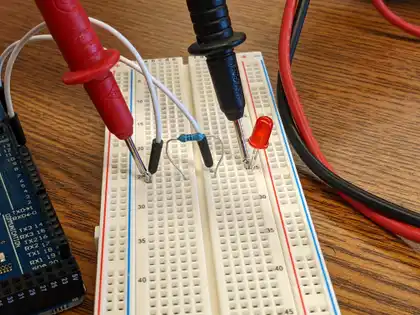
Select a quality digital multimeter (e.g., Fluke 87V, Klein MM700, or equivalent). Rotate the rotary selector switch to the dedicated Diode Test Mode (marked with the triangle-and-line schematic symbol). In diode test mode, the multimeter forces a calibrated test current of approximately 1mA through the component and measures the resulting forward millivolt drop.
- Forward Bias Measurement: Touch the Red Probe (+) to the diode Anode (non-banded end) and touch the Black Probe (–) to the diode Cathode (banded end).
Healthy Benchmark: A high-efficiency Schottky bypass diode must read between 0.300V and 0.450V (300mV to 450mV). Standard silicon diodes (found in vintage panels) will read 0.550V to 0.700V. - Reverse Bias Measurement: Reverse the multimeter leads. Touch the Red Probe (+) to the diode Cathode (banded end) and touch the Black Probe (–) to the diode Anode (non-banded end).
Healthy Benchmark: The multimeter display must read “OL” (Over Limit / Open Loop), confirming zero reverse conduction.
Sandia National Laboratories — PV Power Systems and the NEC (OSTI ID: 808812)
Engineering analysis authored by John Wiles at Sandia underscores that bypass diodes and blocking diodes are exposed to severe atmospheric and lightning-induced voltage surges. For longevity and thermal survival, diode peak reverse voltage (V_RRM) ratings must provide at least a 2.5x to 3x safety margin above the maximum open-circuit voltage of the protected substring. Overcurrent sizing must satisfy NEC Article 690 continuous current multipliers of at least 1.25x short-circuit current to withstand sustained bypass conduction.
Stage 5: Resolving In-Circuit Measurement Ambiguity
Because the bypass diode is wired in parallel with 20 to 24 solar cells, inexperienced technicians can sometimes encounter false low-resistance readings in the reverse direction. In the reverse bias test, the multimeter positive voltage is applied across the series cells. If light strikes the module front face, the internal cell resistance drops, causing the multimeter to display a false leakage reading instead of “OL”. If you observe an ambiguous reading between 0.9V and 1.8V in reverse bias, completely cover the panel face with an opaque tarp. If the reading persists, carefully unclip or desolder one axial lead of the diode from its terminal rail to isolate the diode completely from the cell matrix, then re-test.
Stage 6: Ohmmeter Continuity Verification
Switch the digital multimeter to the Resistance (Ω) setting to verify internal junction integrity. Measure the resistance across the isolated diode:
- Shorted Diode: Displays near zero ohms (0.0Ω to 0.4Ω) in both forward and reverse directions. The continuity beeper sounds continuously. Action: Immediate replacement required.
- Open-Circuit Diode: Displays infinite resistance (Mega-ohms or “OL”) in both forward and reverse directions. Action: Immediate replacement required.
- Healthy Schottky Diode: Displays low forward resistance (typically under 100Ω depending on multimeter test voltage) and infinite resistance (“OL” / >10 MΩ) in reverse bias. Action: Component verified operational.
6. Non-Invasive Sunlight Field Audit: The Voc Drop and Shadow Test
When an off-grid solar installation comprises 20 to 50 roof-mounted or ground-mounted panels, dismounting every module to unseal its junction box is labor-prohibitive. Field engineers utilize a non-invasive two-step sunlight audit to perform preliminary bypass diode array diagnostics in under two minutes per panel without touching a single junction box screw.
Step 1: The Baseline Unshaded Voc Temperature Audit
Perform this audit during midday hours when solar irradiance is steady and exceeds 700 W/m². Disconnect the panel MC4 connectors from the array string to isolate the module under test. Connect digital multimeter probes to the positive and negative MC4 connectors using certified MC4 adapter leads (never force bare metal probes directly into female MC4 terminals, which destroys the internal spring-loaded contact sleeves).
Measure the module open-circuit voltage (Voc_measured). Next, measure the rear backsheet temperature (T_cell) using an infrared thermometer. Calculate the temperature-adjusted expected open-circuit voltage using the manufacturer datasheet temperature coefficient of Voc (β_Voc, typically −0.28% to −0.35%/°C):
V_oc(expected) = V_oc(STC) × [1 + (β_Voc / 100) × (T_cell − 25)]
Compare the measured Voc against the calculated benchmark:
- Normal Tolerance (±3%): All three substrings and bypass diodes are operational.
- Voc Deficit of 33.3% (±2%): Exactly one bypass diode is permanently shorted. For a panel with an expected Voc of 45.0V, a measured reading of 29.5V to 30.5V confirms a single shorted diode.
- Voc Deficit of 66.7% (±2%): Two bypass diodes are shorted. The panel will register between 14.5V and 15.5V.
Step 2: The Controlled Cell Shading Transition Test
While the multimeter remains connected to the panel measuring open-circuit voltage, take an opaque piece of cardboard or dark cloth measuring approximately 160 mm by 160 mm (the exact size of one solar cell). Systematically cover one cell in Substring 1, then Substring 2, then Substring 3.
When you shade a single cell in a healthy panel operating in an open-circuit state, the open-circuit voltage across the panel terminals should drop by approximately 0.35V to 0.5V (the forward voltage drop of the conducting Schottky bypass diode) plus the lost voltage of that specific cell. If shading a specific cell group produces erratic voltage fluctuations, complete voltage collapse to zero, or no voltage change whatsoever, that specific substring diode has suffered open-circuit failure or severe internal bond degradation.
7. NREL Infrared Thermography Standards: FLIR Diagnostic Thresholds
In utility-scale and commercial off-grid arrays, thermal imaging represents the gold standard for rapid bypass diode diagnosis. The National Renewable Energy Laboratory (NREL), in collaboration with Sandia National Laboratories and the SunSpec Alliance, established strict field operating standards for infrared inspection of photovoltaic systems.
National Renewable Energy Laboratory — PV Operations and Maintenance Guide (NREL/TP-7A40-73822 / OSTI ID: 1489002)
NREL O&M best practice guidelines require annual thermal infrared array scans conducted at a minimum solar irradiance of 600 W/m² with irradiance deviation below 100 W/m² and ambient temperature deviation below 5°C. Remote thermal imaging proactively isolates module hot spots, bypass diode failures, and localized junction-box heating. NREL protocols emphasize that while string-level electrical monitoring readily flags shorted diodes due to a 33% voltage drop, open-circuit diode faults can only be detected via thermography or bench-level multimeter diagnostics.
When scanning an operating array with a handheld FLIR or drone-mounted thermal camera compliant with IEC 62446-3 standards, technicians evaluate the following three thermal signatures:
| Thermal Profile | Temperature Delta (ΔT) | Physical Mechanism | Severity & IEC Action |
|---|---|---|---|
| Junction Box Hot Spot | 10°C – 25°C above ambient module | Continuous forward conduction through shorted Schottky diode or loose terminal connection | Class 2 Anomaly: Schedule junction box servicing within 30 days |
| Single-Cell Thermal Hot Spot | 20°C – 45°C above adjacent cells | Localized shading combined with an open-circuit bypass diode; reverse-bias power dissipation | Class 1 Critical: Disconnect module immediately; high fire hazard |
| Uniform Substring Patchwork | 3°C – 8°C cooler or warmer | Entire 20/24-cell group bypassed by shorted diode; cells carry zero current and remain cooler | Class 3 Diagnostic: Confirm with field Voc audit and replace diode |
8. Junction Box Servicing: Schottky Sizing, Soldering and IP67 Sealing
When multimeter diode diagnostics confirm a defective diode, you do not need to replace the entire 300W to 450W photovoltaic panel. With basic workshop tools and proper replacement parts, an off-grid homeowner or technician can replace a failed Schottky diode for under $3 in materials, restoring 100% of the module energy harvest.
Step 1: Selecting the Correct Replacement Schottky Diode
Never replace a solar panel bypass diode with a generic 1N4007 or 1N5408 silicon rectifier. Standard silicon rectifiers have an excessive forward voltage drop (0.8V to 1.1V at high current) and will overheat rapidly inside the sealed junction box. You must install a genuine **Schottky Barrier Diode** rated to satisfy the following electrical criteria:
- Continuous Forward Current (IF): Must be at least 1.25x the module short-circuit current (Isc) per NEC Article 690 guidelines. For modern panels with an Isc of 10A to 13A, select a 15A, 20A, or 30A rated diode.
- Peak Repetitive Reverse Voltage (VRRM): Must exceed at least 2.5 times the open-circuit voltage of the individual substring. For a 20-cell substring generating 13V Voc, a rating of 45V to 50V is standard. Recommended industry part numbers include 15SQ045, 20SQ045, 25SQ045, or 30SQ050.
- Thermal Operating Range: Rated for −55°C to +150°C junction temperature (Tj).
Step 2: Desoldering and Mechanical Extraction
In clamp-style junction boxes, release the stainless steel spring clips using a needle-nose plier and pull the axial diode leads free. In soldered junction boxes, heat the terminal solder joint using a temperature-controlled 60W soldering iron set to 350°C (662°F). Apply copper desoldering braid or a spring-loaded solder sucker to remove molten solder. Use an aluminum alligator clip on the diode lead between the solder joint and the semiconductor body to act as a thermal shunt, preventing excessive heat from damaging the rear module backsheet.
Step 3: Lead Preparation and Polarity Alignment
Using needle-nose pliers, bend the leads of the new Schottky diode to match the exact spacing of the junction box terminal rails. Always bend leads at least 3 mm away from the plastic diode body to prevent internal silicon die cracking. Ensure the Cathode Silver Band aligns precisely with the positive terminal orientation of the neighboring healthy diodes. Reversing diode polarity will create a dead short circuit that permanently destroys the module substring the moment sunlight hits the panel.
Step 4: Precision Soldering and Joint Inspection
Solder the leads using high-grade 60/40 rosin-core leaded solder or SAC305 lead-free solder. Heat the terminal rail and diode lead simultaneously for 3 to 4 seconds, then feed solder until a smooth, shiny concave fillet forms around the entire lead circumference. Allow the joint to cool undisturbed for 30 seconds. Inspect the joint under magnification to ensure zero cold-solder bridges, voids, or thermal crystallization.
Step 5: Environmental Re-Sealing and IP67 Restoration
Moisture ingress inside a solar junction box causes galvanic corrosion of copper busbars and creates electrical tracking paths that arc under high DC voltages. Never use standard acetoxy-cure household silicone (which smells like vinegar); the acetic acid fumes released during curing will corrode the copper ribbon leads within months. Apply an authentic **neutral-cure (oxime or alkoxy) electronic-grade RTV silicone** (such as Dow Corning 737 or MG Chemicals 1035) around the perimeter gasket channel. Snap the junction box lid securely into its locking detents and allow the sealant to cure for 24 hours before reinstalling the module in the array string.
Best Practices for Operation and Maintenance of PV Systems
Author: Andy Walker et al. | NREL, Sandia & SunSpec Alliance (NREL/TP-7A40-73822 / OSTI ID: 1489002). Governs infrared thermography standards, bypass diode failure rates, and annual inspection intervals.
Simulated Performance of Stand-Alone PV Systems
Sandia National Laboratories (SAND87-2379 / OSTI ID: 6207302). Establishes mathematical modeling of array voltage collapse, diode forward conduction losses, and partial shading dynamics.
Facility-Scale Renewable Energy Systems (UFC 3-440-01)
U.S. Department of Defense (USACE, NAVFAC, AFCEC). Mandates severe environmental ingress ratings (IP65/IP67), DC balance-of-system hardening, and junction box terminal maintenance.